The $400 Million Machine Printing Tomorrow's Chips
ASML's newest lithography machine costs $400 million. Its optical projection system alone weighs 12 tons. Intel bought the first one, and 300 ASML engineers flew to Oregon to assemble it in spring 2024. Advanced wafers are trending toward $100,000 each. This is where AI hardware actually comes from.
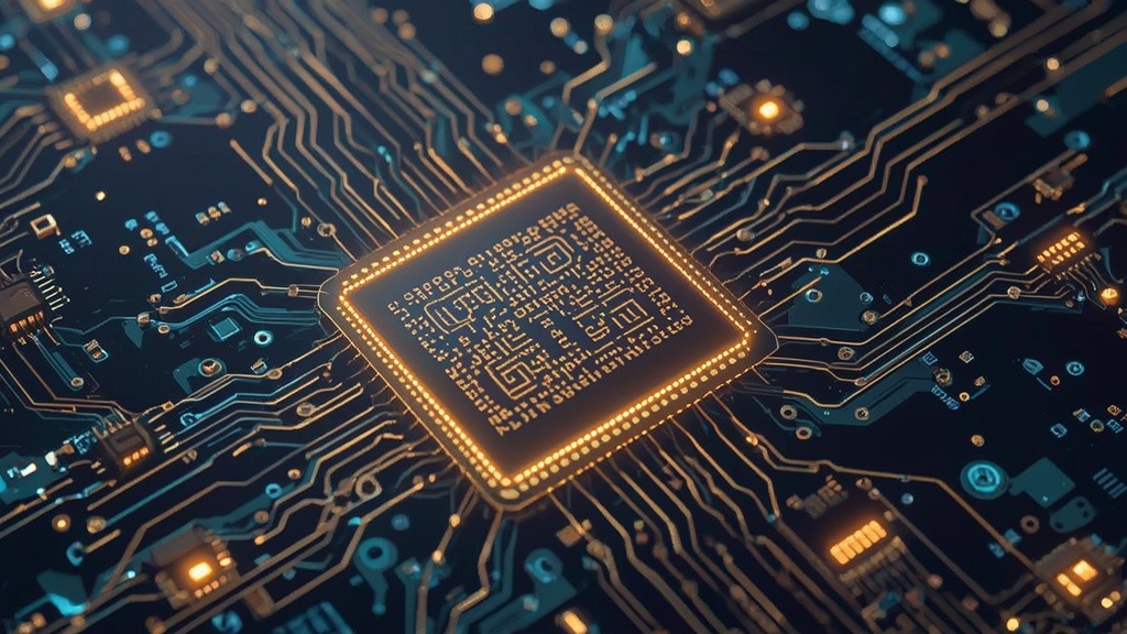
What the Machine Does
The high-NA EUV machine prints circuits at 8-nanometer resolution, the width of roughly 40 silicon atoms. The original EUV machine launched in 2017 at 13 nanometers and cost well over $100 million.
The "NA" stands for numerical aperture. Going from 0.33 to 0.55 cuts transistor size by nearly half and nearly triples density on the same chip area. To get there, the optical projection system grew to 12 tons, seven times heavier than the original EUV optics.
The reticle stage, which positions the chip mask during exposure, accelerates at up to 22g.
How ASML Got Here
EUV R&D took 16 years and cost approximately $10 billion. The result: ASML now produces roughly 90% of all chip-lithography tools worldwide. In 2025, the company sold nearly 50 EUV machines and generated nearly $40 billion in revenue. Its market cap exceeded half a trillion dollars by mid-2026.
The underlying physics uses 13.5-nanometer wavelength light to expose chip patterns. Generating EUV light at production scale is complex enough that no competitor has managed it. The 16-year development timeline reflects that.
The Geopolitics
Starting in 2019, the US pressured the Dutch government to embargo high-end ASML machine sales to Chinese firms. China's government-run response reportedly employs former ASML staff and has built an EUV-like machine occupying an entire lab floor. One floor versus one 12-ton box is a rough measure of the current gap.
Two Challengers
Substrate, a San Francisco startup founded around 2022, is developing x-ray lithography using a compact particle accelerator. The company targets chip production at scale by 2030. Its claimed advantage: finished wafers at $10,000 each, versus the industry trajectory toward $100,000 per wafer.
Lace Lithography, based in Norway, uses energized helium atom beams instead of light. The company claims 0.1-nanometer precision. Machines targeting fabs are expected by 2029 to 2030.
Both companies are pre-production. The history of lithography alternatives reaching manufacturing scale is not encouraging.
What Comes After
ASML is already developing "hyper-NA" EUV with a numerical aperture of 0.75 and 6-nanometer resolution. Potential shipping timeline: second half of the 2030s.
Fab costs are climbing alongside machine prices. Building a single advanced fab now costs up to $25 billion, up from roughly $5 billion in the 2010s. The $400 million machine is one line item in that budget.
Google has deployed TSMC-made TPUs in data centers since 2015. Nvidia's elite AI training GPUs cost $40,000 each. The compute that AI products run on traces back to tools like this one. The $400 million price tag is not the ceiling.
Source: Technologyreview